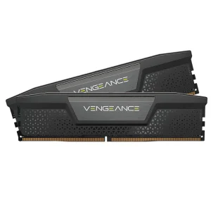
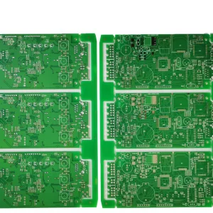
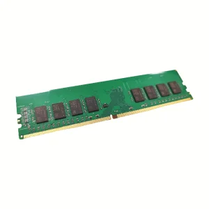
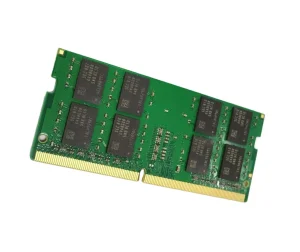
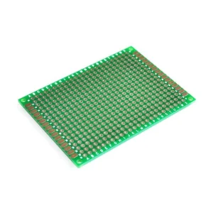
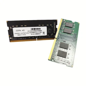
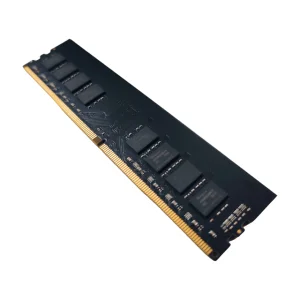
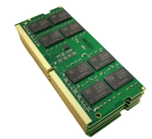
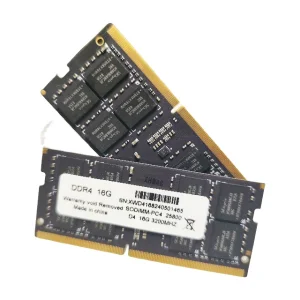
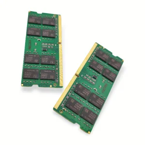
Explore our high-performance electronic components, ranging from OEM double-sided PCBs to DDR4/DDR5 system memory modules built on advanced multilayer technology.
Xeviora Memory Technology (China) Co., Ltd. integrates advanced microelectronics, multi-layer routing layouts, and high-frequency design engineering.
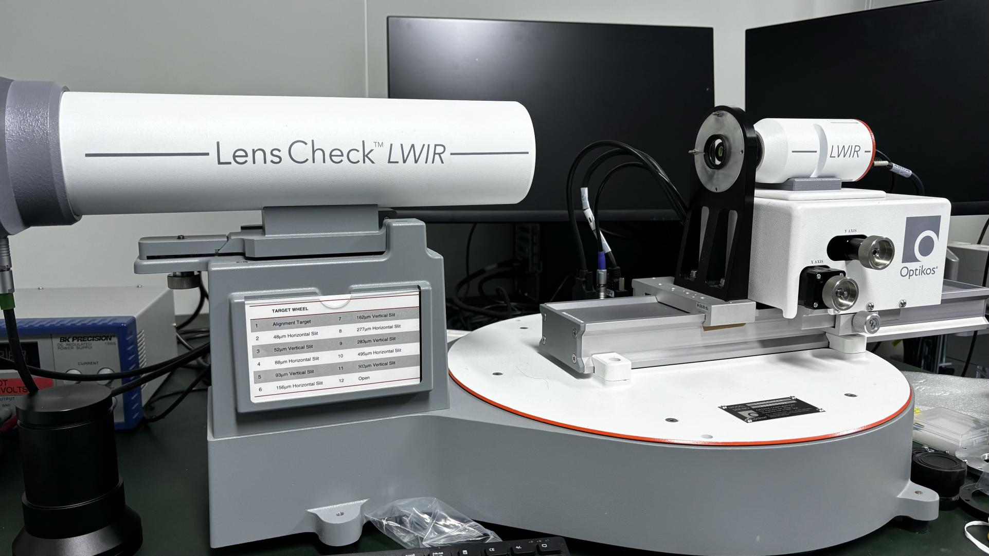
Established in 2017, Xeviora Memory Technology (China) Co., Ltd. has grown from a specialized system layout lab into a robust, high-precision electronic manufacturing brand. Driven by 8 years of international export experience and 12 years of industry engineering expertise, we cater to gaming, industrial, enterprise, and high-demand consumer sectors. Our state-of-the-art testing facility covers 368 square meters, hosting specialized cleanroom spaces optimized for automatic inspection, laser patterning, and advanced reliability validation.
Our commitment to E-E-A-T principles (Experience, Expertise, Authoritativeness, and Trustworthiness) forms the bedrock of our manufacturing capabilities. With an annual export footprint exceeding USD 18 million, our systems support electronic product assembly in North America, Europe, Southeast Asia, the Middle East, and South America. Leveraging our deep technical infrastructure, we manage complex multilayer printed circuit boards and dense signal-routing platforms, partnering with more than 850 global supply chain allies to guarantee component availability and continuous processing efficiency.
High-Density Interconnect (HDI) and signal integrity are essential elements of high-layer-count circuitry.
We process standard stackups from 4 to 32+ layers. Through exact thickness control of dielectric cores and prepregs, we prevent board warpage under thermal strain, ensuring clean trace routing for high-density components.
Utilizing high-speed testing engines, we hold single-ended and differential impedance margins within ±5%. This control optimizes performance for DDR4, DDR5, and PCIe Gen 5 lanes, where signal attenuation must be minimal.
Supporting blind, buried, and stacked microvias (1+N+1 to arbitrary layer connections). Resin-filled via-in-pad plating (VIPPO) avoids solder migration, maximizing trace real estate on miniaturized boards.
In the design of modern electronics, selecting the appropriate substrate material is critical. We use standard FR-4, High-Tg (TG170/TG180), halogen-free laminates, and low-loss high-frequency materials (such as Rogers, Shengyi, or Nelco). High-Tg materials withstand temperatures exceeding 170°C without mechanical degradation, which is critical during Pb-free assembly processes. By controlling the glass transition temperature (Tg) and Coefficient of Thermal Expansion (CTE) along the Z-axis, we prevent barrel cracking and interlayer delamination.
Our localized supply networks enable cost-efficient material sourcing, quick prototyping, and seamless scaling.
Direct proximity to copper-clad laminate (CCL) mills allows us to source copper foils, fiberglass, and resin matrices at lower costs, bypassing global supply delays.
Our facility offers express production tracks. Multilayer PCB prototypes can be fabricated and electrically tested within 48 to 72 hours before shifting to volume runs.
Our production floor features Laser Direct Imaging (LDI) and Automated Optical Inspection (AOI). Laser imaging minimizes trace registration error, down to a tolerance of ±35μm.
By integrating local component networks and advanced assembly plants (PCBA), we simplify the supply chain. Xeviora offers complete turnkey services, covering raw PCB fabrication, component procurement, pick-and-place assembly, and testing. This end-to-end model reduces multi-vendor transit risks, shortens time-to-market, and lowers freight overhead for our global clients.
A reference table outlining our manufacturing tolerances, substrate selections, and surface treatment capabilities.
| Parameter / Metric | Standard Capability | Advanced / Precision Limits |
|---|---|---|
| Layer Count Range | 2 to 16 Layers | Up to 32+ Layers |
| Base Substrates | FR-4, Mid-Tg, Lead-Free Compatible FR-4 | High-Tg (TG180), Rogers (RO4003/RO4350), Polyimide (Flex) |
| Board Thickness | 0.4 mm – 2.4 mm | 0.2 mm – 6.0 mm |
| Minimum Trace Width / Spacing | 3.5 mil / 3.5 mil (0.089 mm) | 2.5 mil / 2.5 mil (0.063 mm) |
| Copper Outer Weight (Thick) | 1 oz – 2 oz | Up to 6 oz (Heavy Copper Power Distribution) |
| Drill Aspect Ratio | 8:1 | 12:1 (For Deep Via Micro-drilling) |
| Surface Finish Options | HASL (Lead-Free), OSP | ENIG (Electroless Nickel Immersion Gold), ENEPIG, Hard Gold Plating |
| Solder Mask Colors | Green, Blue, Black, White | Custom Matte Finishes, High-Reflective White (LED applications) |
From high-capacity server infrastructure to industrial automation networks, our multilayer PCBs support mission-critical applications.
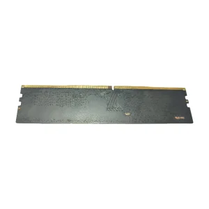
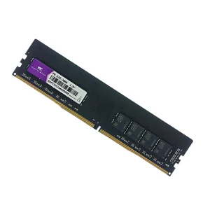
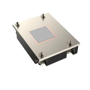
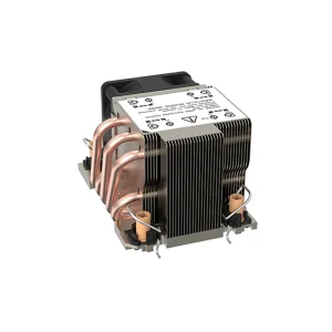
We supply thermal-stable multilayer PCBs designed for dual-channel RAM configurations, passive heatsinks, and AM5 server setups. These boards support reliable power and signal distribution across high-power networks.
Built on thick copper substrates and High-Tg laminates, our industrial control boards handle thermal transitions, electromagnetic interference (EMI), and continuous mechanical vibration.
Certified for critical automotive controls, our high-density interconnect designs manage sensor arrays, radar transceiver modules, and main compute platforms for autonomous driving.
As modern vehicle systems transition to 48V networks and require high-density sensor integration, the demand for reliable multilayer PCBs increases. Standard double-sided boards cannot isolate noise across adjacent signal traces. Using dedicated ground planes, microstrip routing, and strict dielectric control, our multiline stackups minimize cross-talk, keeping signal degradation below measurable limits even at frequencies over 77 GHz.
The PCB market is moving toward high-frequency materials, eco-friendly laminates, and micro-HDI routing.
1. AI Hardware Acceleration & Heat Management: Artificial intelligence networks and dense graphics processors demand massive memory bandwidth (e.g., DDR5 memory and multi-socket platforms). High-speed data processing creates significant thermal loads. To manage this, PCB designs require thick copper planes, high-conductivity ceramic-filled prepregs, and integrated metal cores to dissipate heat away from active silicon.
2. Ecological and Regulatory Compliance: Global regulations (including RoHS and REACH directives) require lead-free electronic assembly. This transition demands high-reflow solder ovens (reaching peaks of 260°C). Consequently, PCB substrates must support high decomposition temperatures (Td ≥ 340°C) to prevent matrix cracking during assembly.
3. Embedded Component Technology: Embedding passive resistors and capacitors directly into inner board layers reduces top-layer footprint requirements. This approach shortens trace loops, lowers parasitic inductance, and improves signal integrity in high-frequency applications.
Direct technical answers to help engineering, procurement, and logistics teams with their PCB projects.
We use Polar Instruments software to run calculations on trace geometry, dielectric constant, and layer heights. Post-fabrication, our QA team tests the boards using Time-Domain Reflectometry (TDR) to verify compliance within +/-5% or +/-10% tolerances.
Electroless Nickel Immersion Gold (ENIG) offers a flat surface finish, which is ideal for fine-pitch BGA packages. The nickel layer provides a strong diffusion barrier for copper, while the thin gold top coat protects the nickel from oxidation during storage.
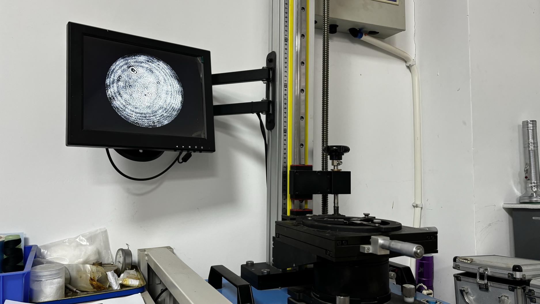
Every multilayer PCB undergoes Automated Optical Inspection (AOI) during the inner-layer stage, followed by 100% electrical testing (via flying probe or test fixture) on finished boards to confirm connectivity matches the netlist.
Yes. We source lead-free laminates, copper foils, and surface-finish chemistry. All products are shipped with compliance documentation verifying restriction limits for heavy metals and hazardous substances.
Via-in-pad plated over (VIPPO) plugs the vias with epoxy resin and caps them with planarized copper. This layout lets designers route signals directly through component pads, lowering parasitic capacitance and optimizing space on HDI layouts.
Standard prototype production takes 3 to 5 days, while medium to high-volume production orders are typically processed within 10 to 15 days, depending on layer counts and specific surface treatment requirements.
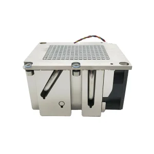
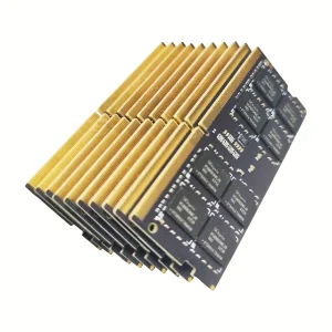
Browse our selection of heavy-duty heatsinks, high-speed RAM products, and custom server cooling hardware.
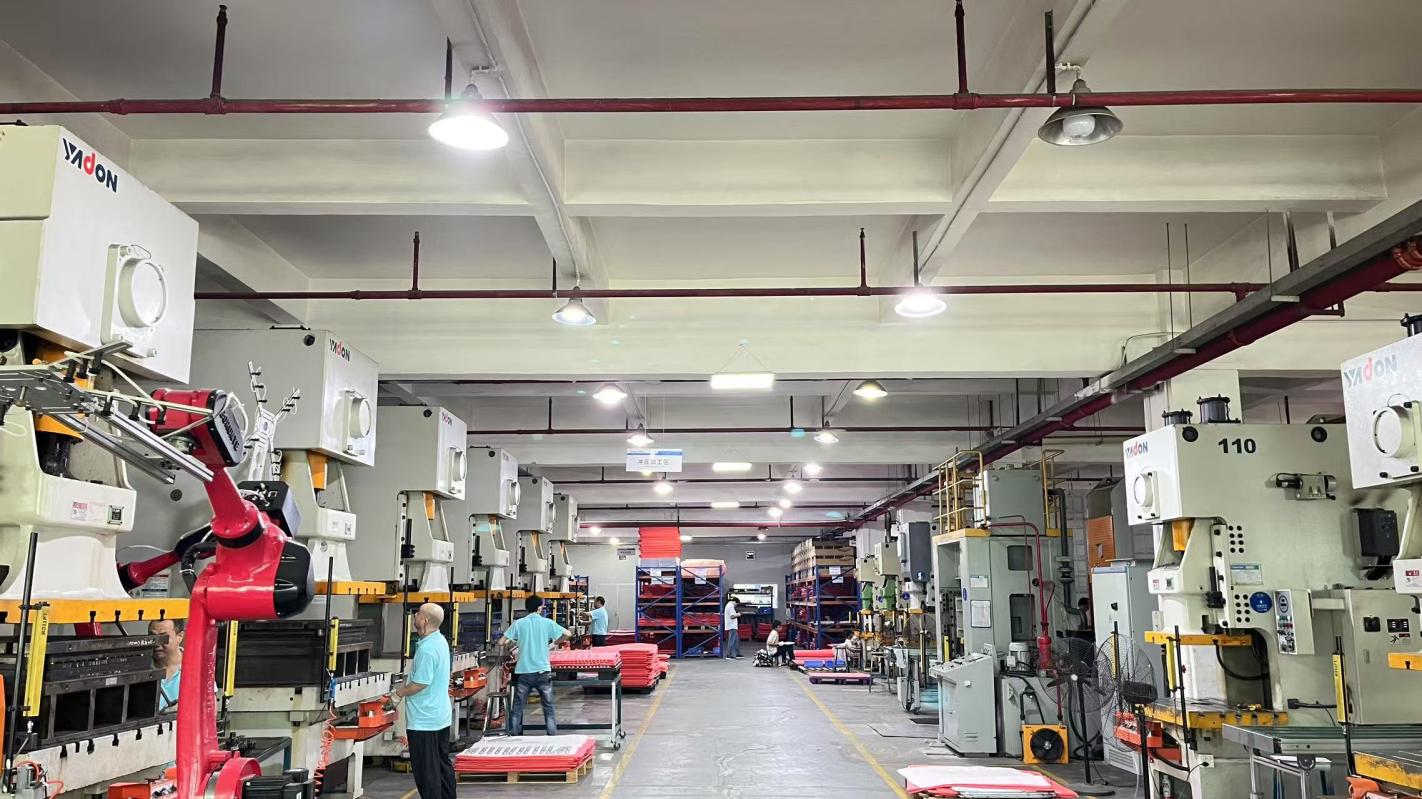
Take a look inside our high-precision fabrication plants, wave soldering units, and inspection workshops.