Engineered for high-reliability computing, advanced robotics systems, and extreme thermal management in Boston's key technological clusters.
The Greater Boston area—extending from the dense innovation centers of Kendall Square in Cambridge to the industrial tech corridors of Route 128—stands as a global epicenter for robotics, aerospace, marine engineering, biotech, and clean energy grid management. High-performance electronic applications developed here demand hardware that can withstand extreme environmental conditions and manage high power densities.
Standard printed circuit boards (PCBs) with standard 1oz copper layers fall short under high electrical loads. Heavy copper PCBs (featuring copper weights from 3oz to over 20oz) are critical for modern power distribution networks, offering unmatched structural reliability and thermal dissipation capabilities. They serve as the backbone for Boston's cutting-edge developments, ensuring high electrical conductivity and robust heat-sinking capabilities in compact spaces.
High current surges in battery systems and DC/DC motor controllers require thick copper paths up to 6oz.
Sealed, sub-sea pressure vessels require internal heat dissipation via heavy copper thermal planes to avoid active cooling failures.
Stable power generation for diagnostic imaging equipment demands low impedance and minimized thermal drift.
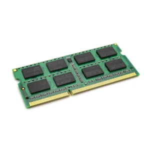
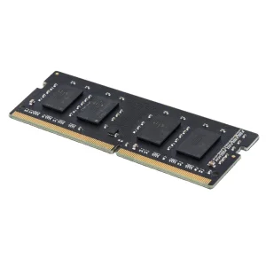
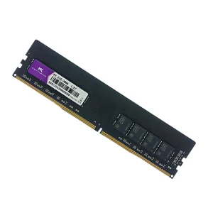
Delivering high-tech substrate fabrication, memory technology, and robust supply chain integration directly to Boston’s engineers and purchasing teams.
Understanding standard design criteria for high-power, thick copper structures ensures seamless DFM (Design for Manufacturing) cycles and reduces prototyping costs.
| Parameter | Standard Range | High-Performance Capabilities | Boston Application Relevance |
|---|---|---|---|
| Copper Weight | 3 oz/ft² - 8 oz/ft² | 9 oz/ft² - 24+ oz/ft² (Custom) | Critical for EV high-voltage chargers and heavy industrial power grids. |
| Base Materials | Standard FR4 (Tg 140°C) | High-Tg FR4, Rogers, Taconic TLY-5, Aluminum Substrates | Ensures high-frequency performance in defense radar and sub-sea communications. |
| Minimum Trace Width / Spacing | 8 mil / 8 mil (at 3 oz) | 12 mil / 12 mil (at 5+ oz) | Prevents dielectric breakdown and short-circuit faults under high loads. |
| Max Board Thickness | 1.6 mm - 2.4 mm | 3.2 mm - 6.5 mm | Adds structural rigidity for heavy industrial vibratory conditions. |
| Surface Finishes | HASL / LF HASL | ENIG, ENEPIG, Immersion Silver, OSP | Improves contact reliability in corrosive oceanographic marine environments. |
Need a custom stackup analysis for your power converter system?
Get Free DFM Engineering ReviewHeavy copper printed circuit boards are the silent workhorses enabling breakthroughs in Boston's target industries.
With Massachusetts targeting carbon neutrality, energy storage installations and microgrid conversion equipment are growing rapidly. Thick copper layers provide high current paths for solar inverters and wind turbine pitch controls.
Boston-based oceanographic startups design AUVs (Autonomous Underwater Vehicles) with extreme space constraints. Eliminating separate bus bars by integrating power and signal planes into thick copper multilayer boards maximizes reliability in deep-water pressure housings.
Contractors in the Massachusetts defense network require Class 3 electronic assemblies. Thicker plating withstands severe thermal shocks and sustains the current density needed for advanced phased-array radar systems.
Ensuring ultra-low signal attenuation, high heat-sinking efficiency, and precise impedance matching for advanced communication channels.
Navigating modern hardware development requires balancing design quality with cost-efficiency. Partnering with a specialized Chinese PCB and memory manufacturing center like Xeviora provides significant benefits:
Direct relationships with top copper laminate manufacturers guarantee high-purity copper foil, reducing procurement costs even during market fluctuations.
Proprietary multi-pass horizontal pattern plating ensures uniform thickness across complex boards, preventing neck-down failures in critical high-power traces.
Rapid transition from initial engineering validation models to high-volume manufacturing, helping companies meet tight market windows.

Designed for deployment under heavy workloads, in harsh environments, and within critical high-frequency transmission systems.
Clear answers to engineering questions about heavy copper circuit boards, thermal dynamics, and international shipping logistics.
A thick or heavy copper printed circuit board features inner or outer layer copper weights of 3 oz/ft² or greater (exceeding 105 µm thickness). Extremely high-power applications may specify "Extreme Heavy Copper," which ranges from 10 oz/ft² to over 24 oz/ft². Standard PCBs, by contrast, typically utilize 1 oz/ft² (35 µm) or 2 oz/ft² (70 µm) copper foils.
Thick copper traces act as highly efficient, integrated heat sinks. Thermal energy generated by high-power semiconductors is conducted directly into the large copper masses, distributing heat evenly across the PCB and dissipating it into the environment or adjacent heat sinks. This design reduces junction temperatures and eliminates the need for bulky, external cooling components.
As copper thickness increases, trace width and spacing rules change. Standard chemical etching requires wider spaces for thicker layers to prevent undercutting. For example, a 3 oz copper layer requires a minimum trace width and space of 8–10 mils, while a 10 oz copper layer requires 20–25 mils of spacing to ensure reliable trace separation.
Heavy copper absorbs a significant amount of heat during assembly. To prevent cold solder joints, engineers should design thermal relief pads on connections to large copper planes. During manufacturing, boards may also require longer dwell times or preheating before wave or reflow soldering.
All fabricated boards comply with IPC-A-600 standards and are manufactured under strict ISO 9001:2015 quality management systems. For critical applications, we support fabrication to IPC-6012 Class 3 specifications, ensuring reliability under extreme stress conditions, alongside UL 94V-0, RoHS, and REACH certifications.
Yes. We specialize in hybrid stackups, combining high-frequency laminates like Taconic TLY-5 or Rogers with heavy copper power distribution cores. This architecture supports RF transceivers, radar systems, and microwave components while maintaining high current capacity.
For urgent engineering prototypes, we offer rapid fabrication services within 7 to 10 days, depending on layer count and copper thickness. Production runs are typically delivered to Logan International Airport or directly to your local facility within 2 to 3 weeks via express air courier.
Connect with our engineering team for stackup calculations, design parameter reviews, and competitive production pricing.
Send Inquiry Now