Direct supply to the Korean industrial corridor. High-reliability components engineered for heavy power applications, thermal management, and computing infrastructure.
South Korea's high-tech industrial architecture—spanning the semiconductor heartlands of Gyeonggi-do (Yongin and Pyeongtaek) to the automotive gigafactories in Ulsan—is undergoing a rapid transition toward high-density power systems.
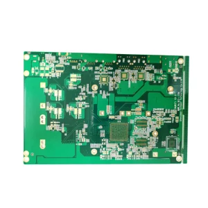
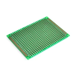
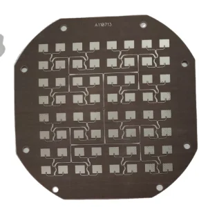
This industrial shift is driven by the mass deployment of electric vehicles (EVs), next-generation fast-charging infrastructure, solar PV power stations, and localized automated manufacturing corridors. Standard printed circuit boards (PCBs) are no longer sufficient; high-power applications require Thick Copper PCBs (also known as heavy copper boards, containing >3 oz/ft² of copper thickness) to manage high currents and disperse thermal energy effectively.
As Korean OEMs strive to shrink the footprint of power distribution units (PDUs), battery management systems (BMS), and variable frequency drives (VFDs), the demand for reliable heavy copper substrates has risen. To remain competitive, Korean buyers are establishing strategic sourcing channels with advanced manufacturing facilities in China that offer rapid turnaround, specialized material properties, and scale.
Core Insight: The shift from traditional multi-board cooling plates to single-board Thick Copper layouts has reduced the overall failure rate in automotive thermal modules by up to 34%, making heavy copper PCBs a key differentiator in the Korean market.
Understanding the balance of copper weight, thermal expansion, and substrate selection to meet rigorous industrial standards.
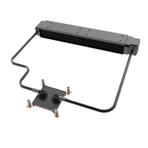
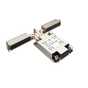
Heavy copper layers serve as integrated heat sinks, directly transferring heat from power semiconductor devices (IGBTs, MOSFETs) through thermal vias, lowering junction temperatures and eliminating the need for bulky external radiators.
By increasing the cross-sectional area of copper traces, heavy copper designs can carry hundreds of amps of current. This keeps the internal temperature rise below safety thresholds established by IPC-2221A standards.
Thick copper plating improves the mechanical strength of connector sites, mounting holes, and multi-layer stack-ups. This provides resilience against thermal shock, cyclic vibrations, and mechanical fatigue in industrial environments.
Optimizing heavy copper designs requires selecting the appropriate base substrate. For instance, pairing heavy copper traces (e.g., 4 oz inner layers) with high-Tg FR-4 (Tg170 or Tg180) prevents resin recession and delamination during high-temperature operations. In environments like automotive under-the-hood systems, metal-clad or aluminum substrate PCBs are paired with heavy copper to improve thermal conductivity.
| Substrate Type | Typical Copper Thickness | Thermal Conductivity | Primary Applications |
|---|---|---|---|
| High-Tg FR-4 (Tg 170/180) | 3 oz – 8 oz | 0.4 – 1.0 W/m·K | Multilayer industrial controls, PDUs, high-voltage switchgear |
| Aluminum Clad (Metal Core) | 2 oz – 6 oz | 1.5 – 3.0 W/m·K | EV Converters, high-power LED systems, solid-state relays |
| Taconic & PTFE Composites | 2 oz – 4 oz | Low Dielectric Loss | RF amplifiers, radar transmitters, high-speed communication |
Procurement departments in major Korean conglomerates face a dual challenge: maintaining rapid local prototyping cycles while securing cost-efficient, high-volume production.
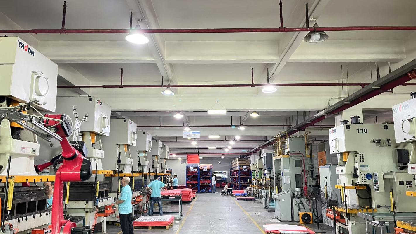
Chinese factories are central to resolving this tension. By utilizing high-capacity automated production lines, these facilities reduce processing costs for thick copper boards, which require prolonged chemical etching and specialized multi-stage electroplating.
Additionally, the geographic proximity between China and major Korean ports (such as Incheon and Busan) enables rapid logistics. R&D teams in Seoul or Daejeon can receive custom-fabricated prototypes in under 5 to 7 days, maintaining project momentum and accelerating time-to-market.
China's manufacturing sector has evolved from high-volume production to smart, automated manufacturing hubs that align with Global E-E-A-T and IPC Class 3 guidelines.
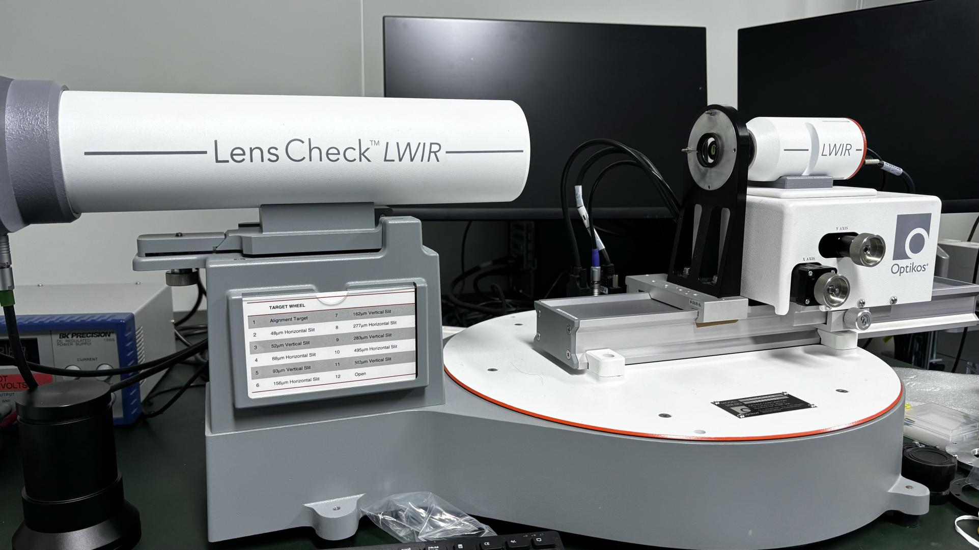
Our facility employs advanced Industry 4.0 principles, integrating Automated Optical Inspection (AOI), high-precision laser direct imaging (LDI), and automated chemical deposition monitoring. This integration ensures trace resolution and consistent copper plating density, even on complex multilayer boards with thick copper tracks.
By leveraging an expansive supply chain of raw materials—including specialized resins, copper foils, and high-frequency laminates—we provide stable pricing and lead times, shielding partners from global logistics bottlenecks and market fluctuations.
Work with an experienced Chinese exporter. We offer custom copper layering, complete reliability testing, and dedicated technical support.
Send Inquiry NowHow thick copper technology supports critical industries throughout South Korea.
Korea's automotive industry relies heavily on heavy copper PCBs to manage the currents generated by lithium-ion battery packs. Thick copper traces on the power distribution board manage high charging and discharging currents, and their high thermal mass helps smooth out temperature spikes during rapid acceleration.
To support green energy goals, KEPCO (Korea Electric Power Corporation) grids integrate utility-scale wind and solar installations. Thick copper PCBs are used in wind power pitch controllers, high-power solar inverters, and power factor correction units to minimize resistance losses and ensure reliable long-term performance.
Korea’s high-speed rail network (KTX) relies on robust power electronics. Engine control modules and track signaling systems use heavy copper boards to withstand continuous current cycles and high temperatures, reducing system maintenance requirements.
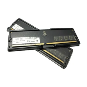
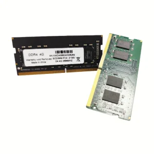
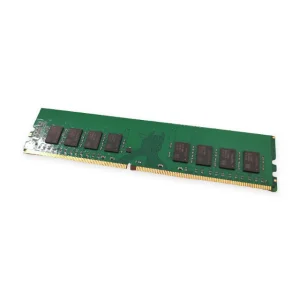
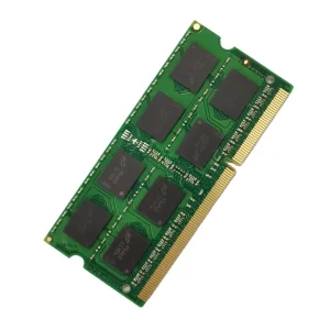
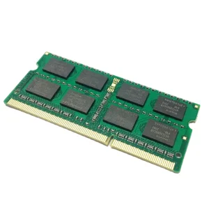
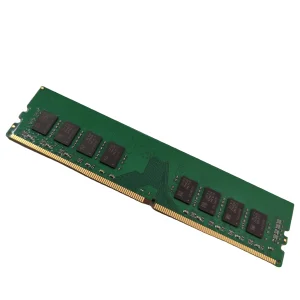
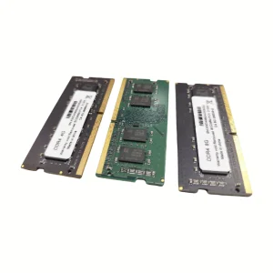
Testing high-performance CPUs, GPUs, and memory modules requires specialized load boards capable of carrying significant current to the device under test (DUT). Multilayer thick copper PCBs provide the low-impedance power distribution required for stable testing.
Established in 2017, Xeviora Memory Technology (China) Co., Ltd. has expanded its high-performance electronic solutions to support the global industrial sector, specializing in thick copper substrates and memory modules.
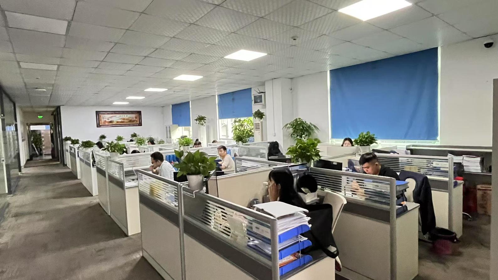
Our manufacturing facility is equipped with modern production and testing systems to ensure consistent quality and reliable performance. Supported by 8 years of export experience and 12 years of industry expertise, we deliver products that meet international standards.
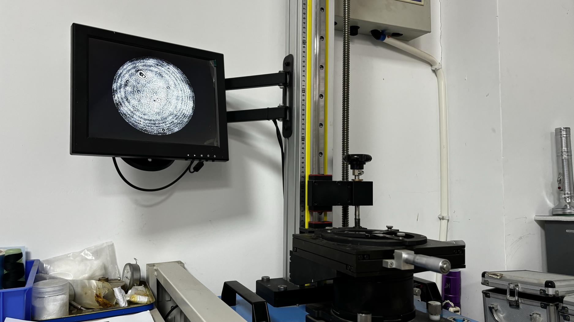
Our quality management system spans incoming material inspection, in-process quality control, and final product testing. All products undergo automated functional testing, compatibility verification, performance validation, and thermal aging tests before shipment to ensure high reliability.
As a manufacturer with OEM and ODM capabilities, we collaborate with over 850 supply chain partners worldwide, enabling efficient sourcing and flexible production. Our primary clients include industrial system integrators, technology brands, and system builders.
Customization Services: We offer flexible customization options, including specialized substrate materials, trace layout consulting, copper weight optimization, and comprehensive testing validation tailored to your specifications.
Our R&D team of 128 engineers continually invests in manufacturing processes and material sciences. This enables us to consistently supply advanced thick copper layouts and memory modules to major manufacturing hubs across Korea, Southeast Asia, Europe, and North America.

Addressing the common questions raised by Korean procurement managers and engineers when sourcing thick copper PCBs from China.
A thick copper (or heavy copper) PCB generally features copper conductors with thicknesses ranging from 3 oz/ft² to over 10 oz/ft². Our facility can fabricate multi-layer configurations with inner layer copper thicknesses up to 8 oz and double-sided structures up to 12 oz, depending on the trace width and spacing requirements.
Thicker copper foils require longer exposure to chemical etchants, which can lead to lateral etching (undercutting). We minimize this effect by adjusting the trace compensation in our CAM processes, using LDI (Laser Direct Imaging) for precise dry film placement, and maintaining chemical balance in our high-pressure spray etching systems.
Yes, we specialize in manufacturing hybrid stack-ups. We laminate heavy copper cores with high-frequency substrates (such as Taconic TLY series or Rogers composites) using optimized curing temperatures and pressures. This ensures robust bond strength without compromising dielectric properties.
Our standard test sequence includes Thermal Shock Testing, Micro-sectioning Analysis to inspect plating thickness in vias, Solderability Testing, and IPC Class 3 compliant flying probe electrical testing. Upon request, we also provide detailed test reports and Certificate of Conformance (CoC) documents.
We offer both air express (via DHL, FedEx, or SF Express) and sea freight (shipping from Shenzhen or Shanghai ports directly to Incheon or Busan). Typical air transit takes 2 to 4 working days, while sea freight averages 5 to 7 days, providing reliable delivery timelines for both prototypes and mass production runs.
We offer complete OEM/ODM support, including customized stack-up layouts, materials validation, thermal simulation assistance, impedance calculations, and options for private labeling and customized packaging.
Browse our selection of server-grade memory modules, high-frequency substrates, and thermal management hardware engineered for industrial markets.