High-performance processing modules and controller architectures essential for managing high-precision ultraviolet optical sensors and automation systems in the Berlin region.

Berlin has established itself as one of Europe’s premier clusters for optical technologies, microelectronics, and life sciences. The scientific hub of Berlin-Adlershof, combined with dynamic biotechnology networks, has created an unprecedented local demand for high-reliability deep ultraviolet (UV) solid-state light sources. In particular, the spectrum spanning 270nm to 410nm packaged in standard 3535 ceramic packaging represents the bleeding edge of precision sterilization, photochemical curing, and chemical analysis.
Local industries require robust optoelectronic systems that align with strict EU directives. Berlin’s academic institutions, clinical laboratories, and municipal water purification facilities are rapidly transitioning from traditional low-pressure mercury vapor lamps to solid-state 3535 UVC LED modules. These compact, mercury-free emitters provide key advantages: instant-on capabilities, dynamic tuning, longer operational lifespans, and zero toxic chemical waste, matching Germany’s strict environmental and safety guidelines.
Understanding why the 3535 package represents the global standard for heavy-duty UV output, and how thermal engineering directly impacts spectral efficiency.
The 3.5mm x 3.5mm footprint represents a high-density packaging design that utilizes aluminum nitride (AlN) ceramic substrates. Ceramic packaging is critical because UV wavelengths—especially under 300nm—rapidly degrade standard organic epoxy resins used in low-cost SMD LEDs. The inorganic nature of the AlN carrier, combined with a high-transmittance quartz glass dome lens, ensures zero degradation under intense UV radiation.
Additionally, the thermal path must be meticulously managed. High-output UVC LEDs operate at low external quantum efficiencies (EQE), meaning a significant portion of input electrical power is converted directly into heat. The AlN substrate provides a thermal conductivity rating exceeding 170 W/m·K, transferring heat directly away from the epitaxial junction to the heat sink, preserving the target wavelength and extending the L70 lifetime of the chip.
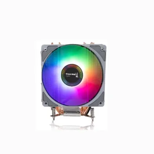
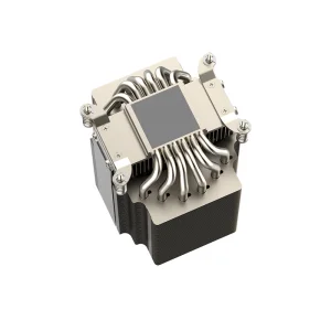
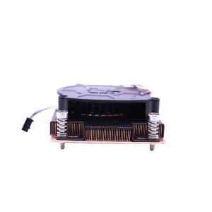
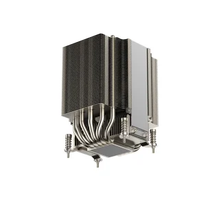
For systems operating in Berlin's demanding scientific laboratories, constant light engine output is non-negotiable. Wavelength shift (red-shifting or broadening) caused by junction overheating can render a calibration system inaccurate or lower a water sterilizer's disinfection rate below its target log-reduction level. That is why our optoelectronic solutions are paired with custom-designed, high-heat flux copper and aluminum coolers.
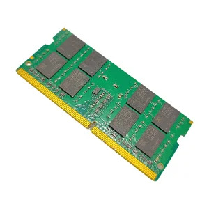
Integrating high-efficiency heatsinks with precise computer control modules (such as our high-speed DDR4/DDR5 system controllers) allows automated feedback loops to dynamically adjust LED currents based on real-time temperature telemetry, preventing junction fatigue.
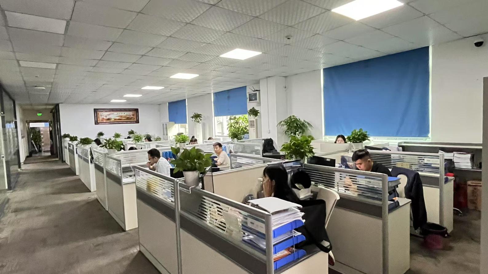
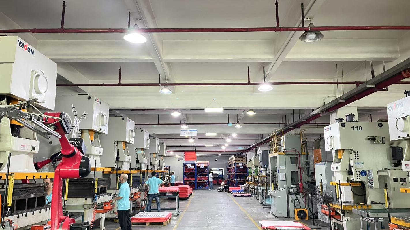
Xeviora Memory Technology (China) Co., Ltd. is a leading manufacturer of high-reliability semiconductor control modules, specialized SMT assembly solutions, and precision optoelectronic components. Our manufacturing facility spans an advanced production floor equipped with state-of-the-art automated placement machines, multi-zone reflow ovens, and 3D Automatic Optical Inspection (AOI) technology.
By operating with a robust network of over 850 global supply chain partners, we ensure immediate availability of premium grade components. Our R&D team of 128 expert engineers works alongside 46 dedicated quality inspectors to execute strict quality control procedures. All components are subjected to rigorous burn-in tests, functional cycling, and thermal stress tests to verify adherence to European safety and performance standards before shipment to Berlin.
Our ultra-clean SMT assembly line guarantees void-free soldering of 3535 UVC LEDs onto custom metal core PCBs.

Guaranteeing complete regulatory alignment with German industrial codes and seamless delivery from factory floor to Berlin logistics hubs.
Our manufacturing and assembly protocols strictly conform to CE Mark, RoHS Directive 2011/65/EU, and REACH requirements. All optoelectronic PCBs, including the critical 3535 package configurations, use lead-free solder pastes and zero hazardous materials, ensuring hassle-free clearance through German customs and alignment with municipal tender requirements in Berlin.
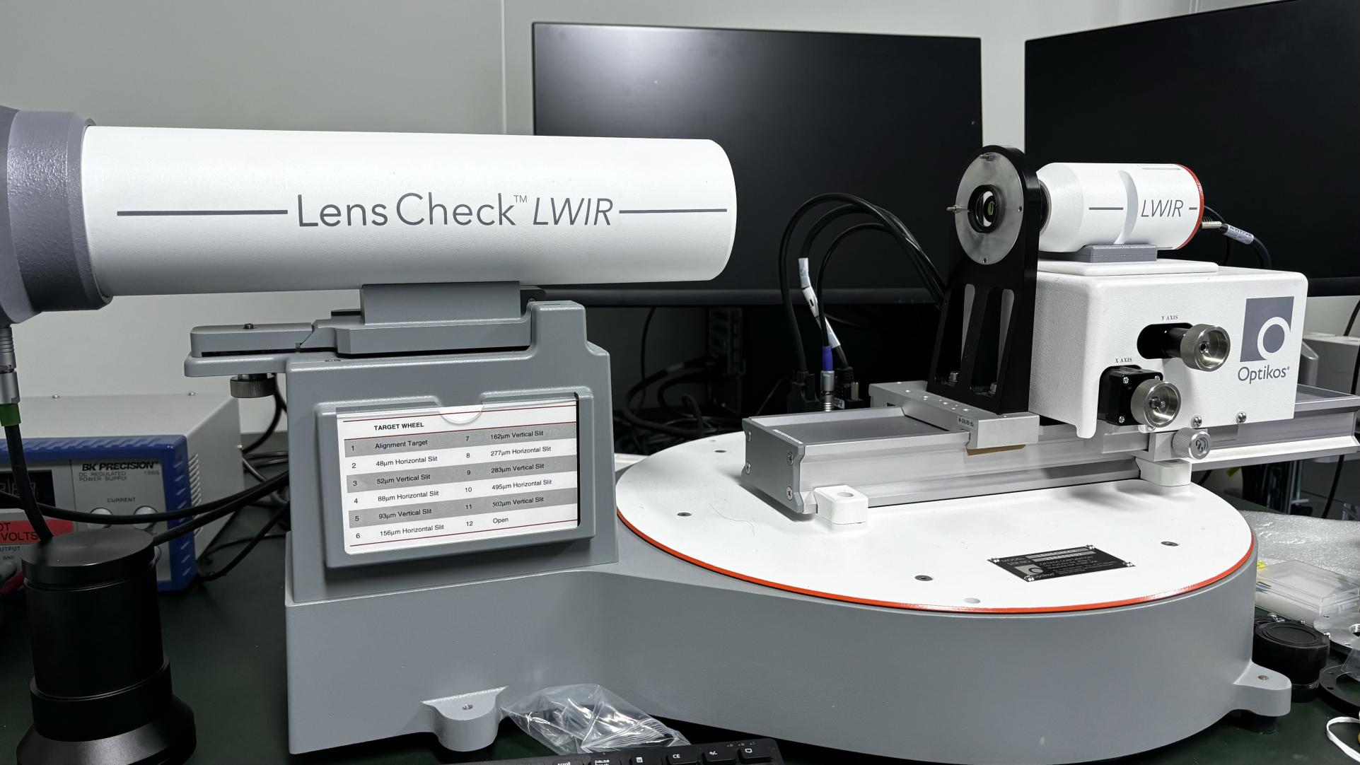
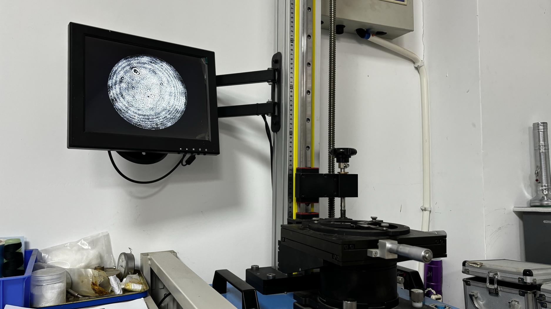
We supply verified radiometry reports with every shipment. Utilizing advanced spectroradiometers, we document absolute irradiance, peak emission wavelength accuracy (to within ±2nm), and spatial distribution. This compliance matches safety standards for skin and eye safety under DIN EN 62471 for lighting systems deployed in public German spaces.
Through our established shipping networks, we provide door-to-door air freight delivery to Berlin-Brandenburg Airport (BER) or major industrial freight depots in Berlin. We handle custom documentation, export clearances, and provide localized support with custom tariff codes (HS Codes) for optoelectronics and controller systems.
High-efficiency thermal management units and precision driver PCBA assemblies engineered to maximize the operational lifespan of 270nm-410nm UVC arrays.
Get authoritative insights regarding 270nm-410nm 3535 UVC LED implementation, optical properties, and manufacturing standards for Berlin buyers.
The 3535 ceramic package provides high thermal conductivity (using Aluminum Nitride substrates) and excellent resistance to degradation from short-wavelength ultraviolet radiation. Unlike plastic SMD packages, it does not yellow or crack under constant UV exposure, ensuring a longer product life and reliable radiant flux.
A 275nm LED is completely mercury-free, instantly starts without preheating, and has a smaller footprint. This allows for more compact and flexible device designs. Furthermore, it operates on low-voltage DC power, making it safer and easier to integrate with electronic control systems in water and air disinfection units.
UVC LEDs convert over 90% of electrical energy into heat instead of light. If this heat is not quickly dissipated, the junction temperature will rise, causing a decrease in optical output power, wavelength drift, and a shorter lifespan. Using high-conductivity heatsinks is essential to maintain target efficiency.
Industrial UV curing of inks, adhesives, and coatings typically uses UVA wavelengths from 365nm to 405nm. Photochemically active initiators in these materials react rapidly under high-intensity UVA radiation, curing and hardening the material in seconds.
Yes, our light engines and modules are tested in accordance with DIN EN 62471 to evaluate optical safety hazards. We provide safety data and specify exposure limits to help Berlin system designers integrate appropriate shielding and safety interlocks.
Yes. Through our SMT production line and design team, we offer complete OEM/ODM services for custom driver boards. This includes metal core PCB layouts, thermal simulation, current-regulation drivers, and integration with control processors.
Standard custom samples are completed within 7 to 10 days. Mass production orders generally ship within 15 to 25 days depending on the volume. We offer express air transport to Berlin-Brandenburg Airport (BER) to ensure fast delivery.
Every batch of LEDs is measured using an integrating sphere and spectroradiometer. We supply detailed documentation showing peak wavelength, full-width at half-maximum (FWHM), and total radiant flux for all deliveries.
When operated under proper thermal conditions (with a junction temperature kept below 60°C), our premium 3535 UVC LEDs have an L70 lifetime exceeding 10,000 to 15,000 hours, depending on the specific current settings.
Yes, we support local research institutes, universities, and technology startups in Berlin by offering flexible minimum order quantities (MOQs) for prototype testing and validation phases.