In high-power electronics, standard PCBs (utilizing 0.5oz to 1oz copper weights) quickly reach their thermal and electrical limits. Thick copper circuit boards, defined primarily by copper weights ranging from 3oz/ft² to over 20oz/ft² (or trace thicknesses exceeding 105µm up to 700µm), represent the foundation of modern high-power electrical distribution. By utilizing heavy copper layers, design engineers can safely route huge currents while simultaneously utilizing the copper traces as integrated heat sinks.
The fundamental physics of heavy copper circuits trace back to the relationship between copper cross-sectional area, current density, and temperature rise ($\Delta T$). Increasing the thickness of the copper deposition rather than simply widening the trace allows engineers to retain highly compact footprints while averting localized thermal runaway. Furthermore, these thick copper cores are laminated with high-Tg (glass transition temperature) FR4, PI (Polyimide), or ceramic-filled substrates to guarantee structural integrity under continuous thermal stress.
Selecting a reliable thick copper PCB supplier requires evaluating key technical dimensions. Standard board shops cannot handle the complexities of thick-film electroplating, differential etching, and multi-stage solder mask application. A true tier-1 supplier must satisfy the following critical criteria:
The ability to control the etching factor in heavy copper layers (avoiding excessive undercutting of tracks) ensures exact trace width and spacing parameters.
Multiple coats of liquid photoimageable (LPI) solder mask must be applied via screen or spray printing to properly fill the deep valleys between thick copper runs without leaving voids.
Suppliers must supply high-Tg materials (Tg > 170°C or Tg > 180°C) coupled with high thermal conductivity to withstand severe reflow cycles and high operational temperatures.
| Copper Weight (oz) | Thickness (µm) | Min Trace Width (mil) | Min Clearance (mil) | Primary Industrial Application |
|---|---|---|---|---|
| 3 oz | 105 µm | 8 mil | 8 mil | Industrial Automation, LED Drivers, Solar Inverters |
| 4 - 6 oz | 140 - 210 µm | 12 mil | 12 mil | EV Battery Management Systems, Power Grid Inverters |
| 8 - 12 oz | 280 - 420 µm | 18 mil | 20 mil | Heavy Machinery Controls, Traction Converters, Rail Transit |
| 15+ oz | 525+ µm | 30 mil | 30 mil | Military Radars, Heavy Power Distribution Systems, EV Fast Chargers |
As global industries transition toward electrification and higher energy densities, the demand for thick copper circuit boards has skyrocketed. In the Renewable Energy Sector, wind turbines and solar photovoltaic systems utilize central inverters that convert direct current (DC) into alternating current (AC). These inverters require heavy copper boards to handle high current loads while maintaining thermal stability.
In the Automotive and EV Ecosystem, vehicle electrification depends on battery management systems (BMS), high-voltage DC-DC converters, and rapid-charging ports. Utilizing thick copper substrates allows design engineers to place power components and control systems onto a single substrate, reducing cable wiring harnesses, minimizing assembly errors, and lowering overall system weight.
Lastly, the modernization of Telecommunications & High-Performance Computing (HPC) has prompted designers to implement hybrid boards. These boards combine high-frequency laminates for signal integrity with thick copper layers for localized high-power distribution. This approach helps handle the extreme transient currents drawn by high-power AI processors.
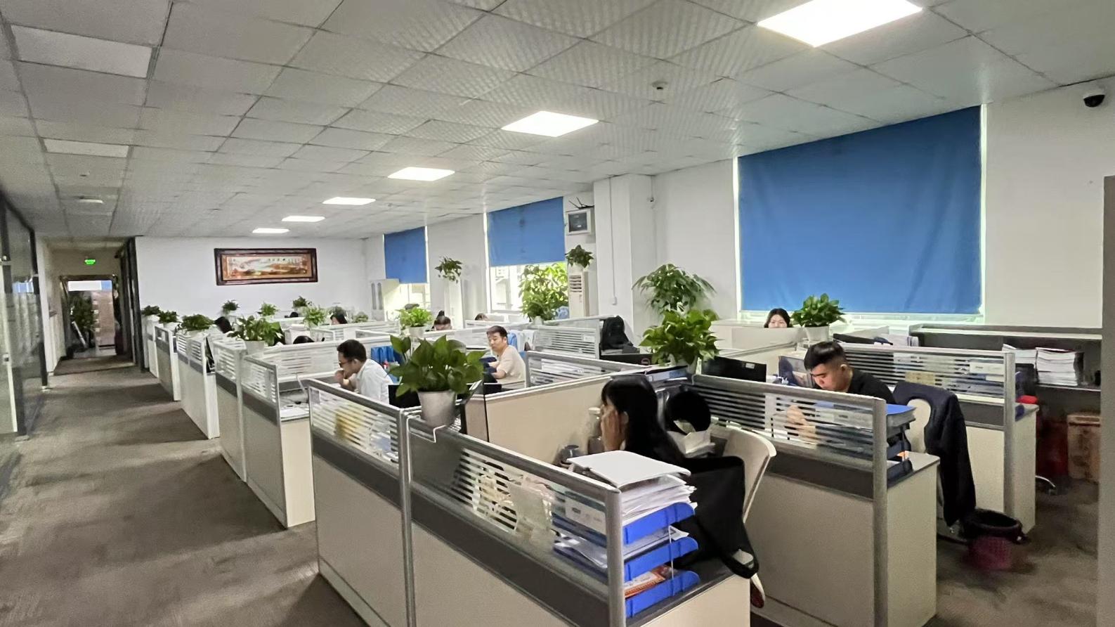
Originally established in 2017, Xeviora Memory Technology (China) Co., Ltd. has established itself as an innovative high-performance electronics manufacturer. While our company is globally recognized for its DDR5 gaming memory, industrial-grade storage solutions, and advanced server memory architectures, we have concurrently developed deep expertise in high-power PCB fabrication and high-conductivity thermal solutions. Our state-of-the-art facility features advanced production and testing lines to support both consumer microelectronics and high-power industrial assemblies.
With an annual export revenue exceeding USD 18 million and supported by a global logistics network, Xeviora serves prominent clients across North America, Europe, Southeast Asia, the Middle East, and South America. Leveraging 8 years of export experience and 12 years of industry expertise, our team provides comprehensive OEM and ODM support. This allows us to work closely with over 850 global supply chain partners.
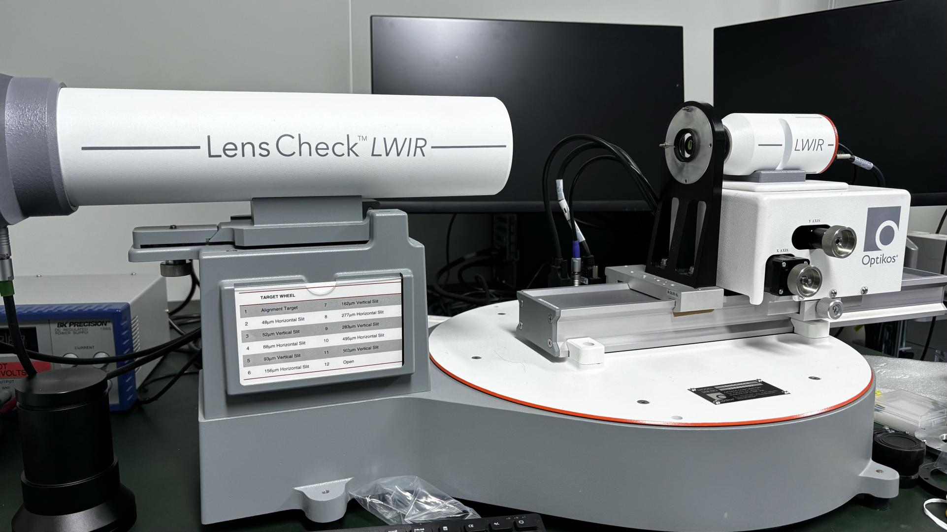

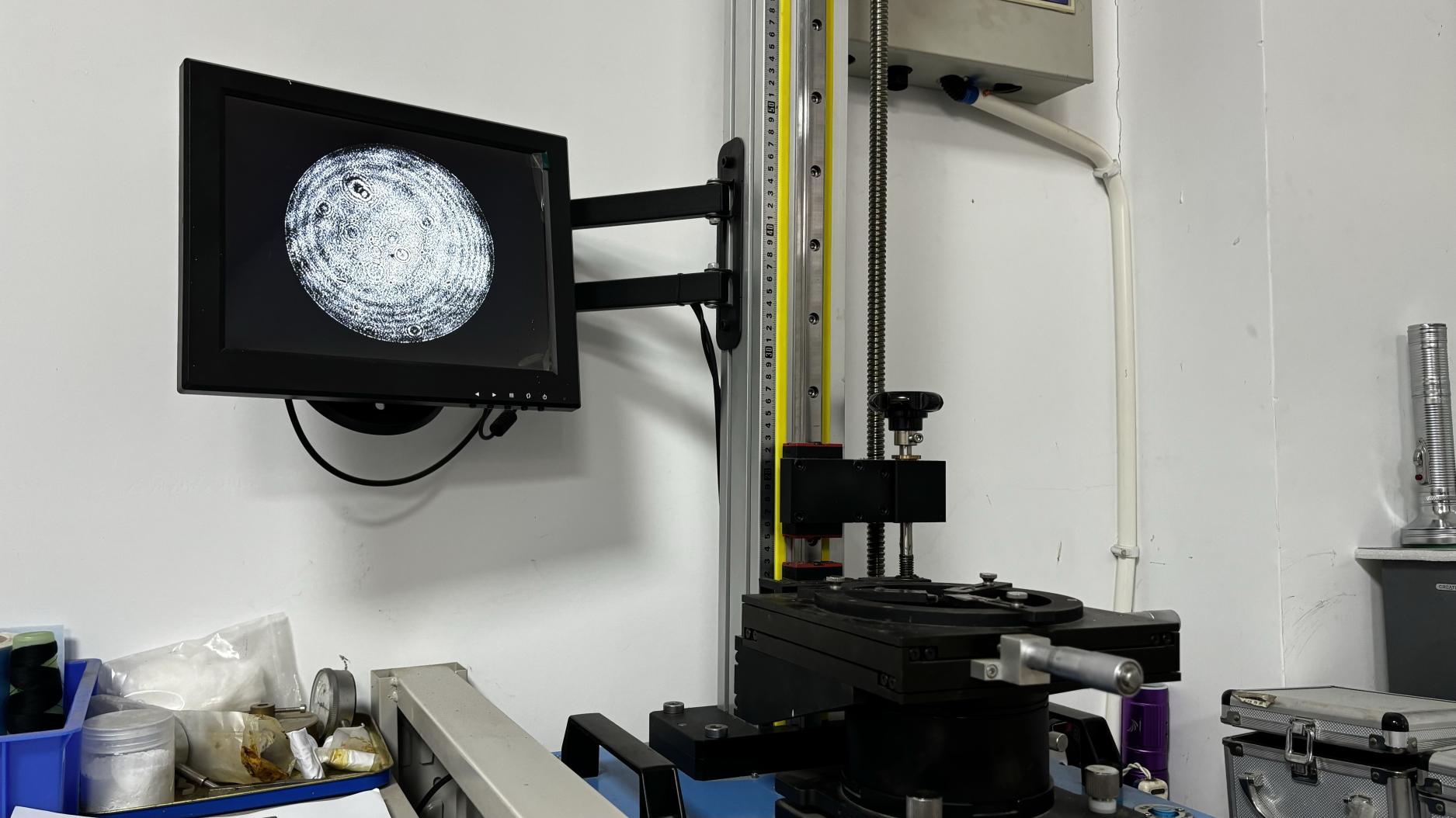
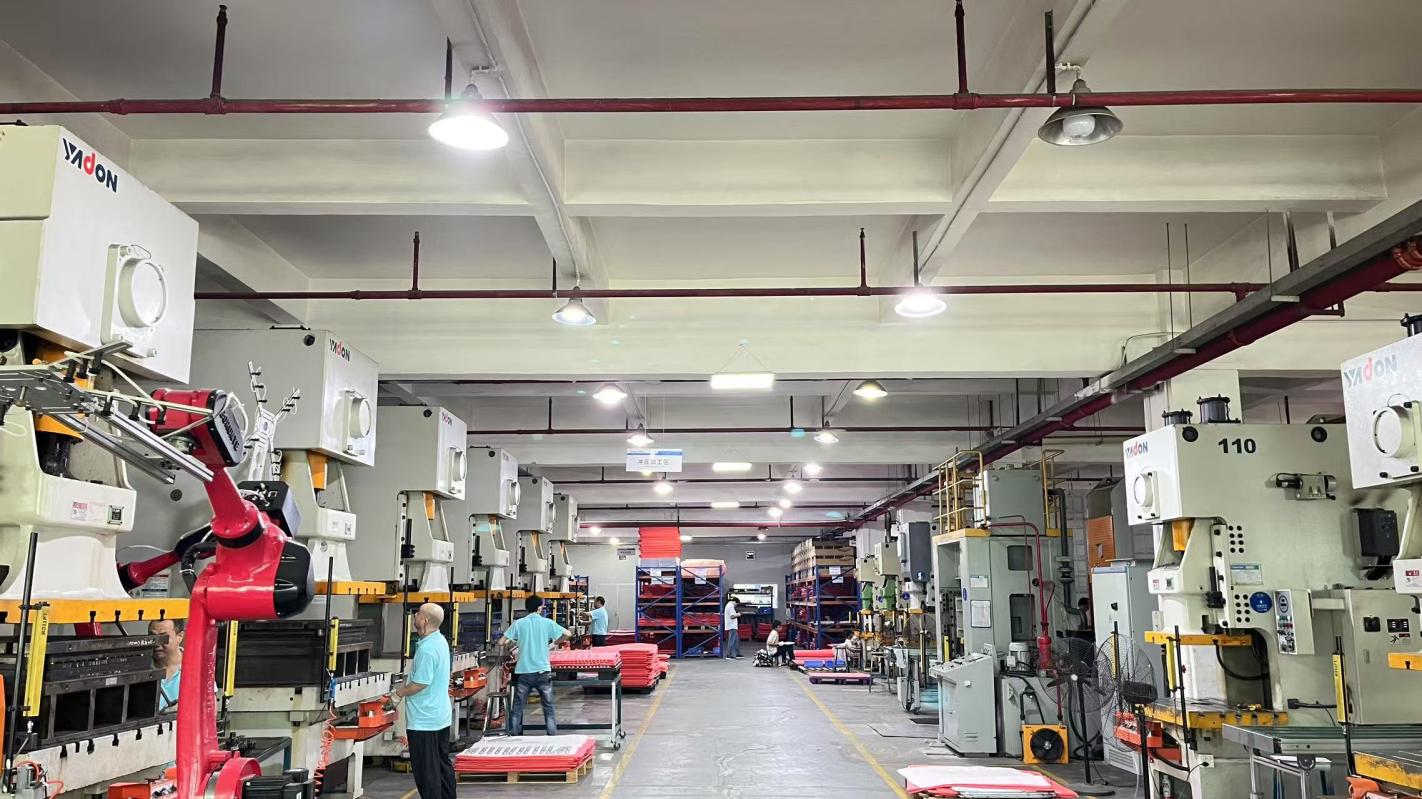
Our manufacturing facility features automated optical inspection (AOI), high-precision flying probe testing, and specialized electroplating lines designed for thick copper circuits and multi-layer stack-ups. Our engineering team, which includes 128 dedicated R&D professionals, continuously develops specialized substrates. This includes metal-clad PCBs, high-frequency laminates, and thick copper boards capable of handling currents over 300 Amps.
Quality assurance remains our top priority. We employ 46 dedicated quality inspectors to monitor each step of the manufacturing process, from incoming raw copper laminate inspection to solderability validation and thermal stress testing. We check every heavy copper board for dielectric breakdown, trace profile accuracy, and thermal shock resistance. This strict process ensures reliable performance in demanding operating environments.
Operating globally requires strict compliance with regional standards and safety codes. In the United States, heavy copper boards designed for power distribution must meet UL 796 standards for printed wiring boards, as well as IPC-6012 Class 3 (High Reliability Electronic Products) requirements. Our engineering team designs these boards to maintain safe clearances and prevent arcing, helping clients secure UL certification for their end systems.
In the European Union, compliance with RoHS (Restriction of Hazardous Substances) and REACH directives is mandatory. We ensure that our thick copper boards utilize lead-free surface finishes, such as Electroless Nickel Immersion Gold (ENIG), Immersion Silver, or Organic Solderability Preservatives (OSP). Additionally, we source our materials from conflict-free smelters to maintain full traceability and align with global environmental, social, and governance (ESG) standards.
For industrial deployments in humid or highly corrosive environments (such as offshore wind farms or coastal solar grids), we apply specialized conformal coatings and thick solder mask barriers. These protective layers prevent copper oxidation and electrochemical migration, extending the operational life of the boards.
The next generation of high-power circuit design is moving toward integration and hybridization. Rather than building entire boards with uniform thick copper layers, which increases weight and processing costs, advanced fabricators are shifting toward embedded copper busbars. By selective embedding of solid copper plates within a standard multi-layer PCB, designers can route logic signals on the outer layers while handling high currents internally.
Additionally, high-temperature operations (reaching above 200°C) have driven the adoption of ceramic-based and metal-clad substrates. These materials feature matching coefficients of thermal expansion (CTE) with power silicon components, helping prevent micro-cracks in solder joints. Xeviora's R&D division is currently developing 20oz copper laminates combined with liquid-crystal polymers (LCP). This combination helps meet the thermal and electrical performance demands of aerospace applications.