Top 10 Laser Cutting Stencils Manufacturer & Factory

Precision-Engineered Micro-Aperture SMT Stencils Driving Global High-Density Semiconductor Assembly & PCB Yield Rates

Featured Advanced SMT & Memory Infrastructure

Executive Whitepaper: The Critical Role of High-Precision Laser Cutting Stencils

In the contemporary electronics manufacturing service (EMS) industry, surface mount technology (SMT) is moving toward ultra-fine pitch components, 01005 (0402 metric) chips, and complex multi-level micro-BGAs. In this context, laser cutting stencils are no longer mere steel plates with holes; they are complex mechanical tools engineered to control the deposition of solder paste down to the picoliter level. Precision in stencil fabrication directly correlates with the final yield rate of printed circuit board assemblies (PCBA). Statistical analyses show that up to 70% of all SMT defects—such as bridging, voiding, and insufficient solder—originate from the paste printing process. Choosing an elite stencil manufacturer is not a purchasing decision; it is a yield optimization partnership.

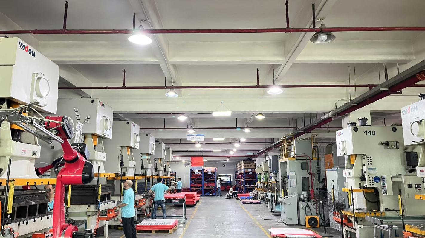
Xeviora Memory Technology (China) Co., Ltd., established in 2017, bridges the gap between memory module engineering and microscopic stencil design. Operating a state-of-the-art facility featuring 368 square meters of high-precision stencil processing cleanrooms alongside our core memory manufacturing assets, we process advanced PCBAs and stencils under strict international standards. Supported by an experienced R&D team of 128 engineers and 46 dedicated quality control inspectors, we deliver optimized stencil apertures tailored to the thermodynamic behavior of modern solder alloys.

12+ Yrs

Industry Expertise

128

R&D Engineers

46

QC Inspectors

$18M+

Annual Export Value

Aperture Physics & Material Technology Map

Fine-Grain Stainless Steel

Engineered using premium, ultra-fine crystalline steel alloys (grain size < 5 µm). Reduces micro-fracturing on the walls during high-speed fiber laser cutting, offering up to 20% smoother aperture walls compared to standard industrial-grade SUS304 sheets.

Hydrophobic Nano-Coating

Our proprietary polymeric organosilicon nano-coatings repel both water and oil-based flux systems. This minimizes solder paste residue buildup inside the micro-apertures, reducing cleaning cycles from every 3 prints to every 30 prints, saving solvent and cycle time.

Tapered & Trapezoidal Geometry

Applying state-of-the-art optical focus control during the laser cutting process creates a 1 to 2-degree trapezoidal aperture opening wider on the PCB contact side. This optimized structure enhances the solder paste transfer efficiency (TE) for ultra-fine pitch QFNs and BGAs.

Macro Industry Applications & Yield Engineering Solutions

Automotive Electronics (AEC-Q100)

In high-reliability automotive environments, solder joint voids can cause sudden system failures. Our stencils feature optimized cross-hatch micro-venting designs in massive heat-slug apertures to reduce gas entrapment under power transistors, keeping void ratios below 10%.

Enterprise Servers & DDR5 Modules

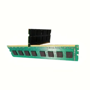
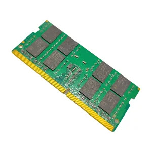
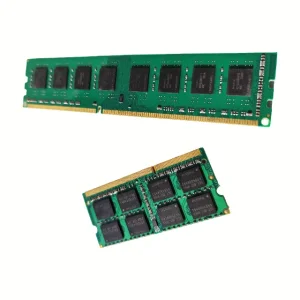
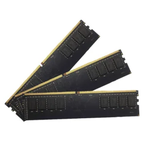
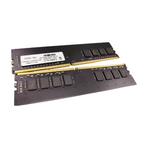
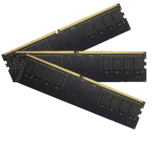
High-density DDR5 DIMMs require stencil thickness variations across the substrate. Our multi-level step-up and step-down stencils are manufactured via ultra-precise electrochemical etching or dual-foil welding, guaranteeing optimal solder thickness at fine-pitch memory controllers.

Consumer Devices & Micro-BGA

Modern mobile systems depend on ultra-miniature 03015 resistors and 0.3mm-pitch BGAs. We leverage femtosecond lasers to create sub-50-micron apertures with high positional tolerance, ensuring perfect registration on complex multi-layer substrates.

China Factory 4.0: Supply Chain Resilience & Manufacturing Infrastructure

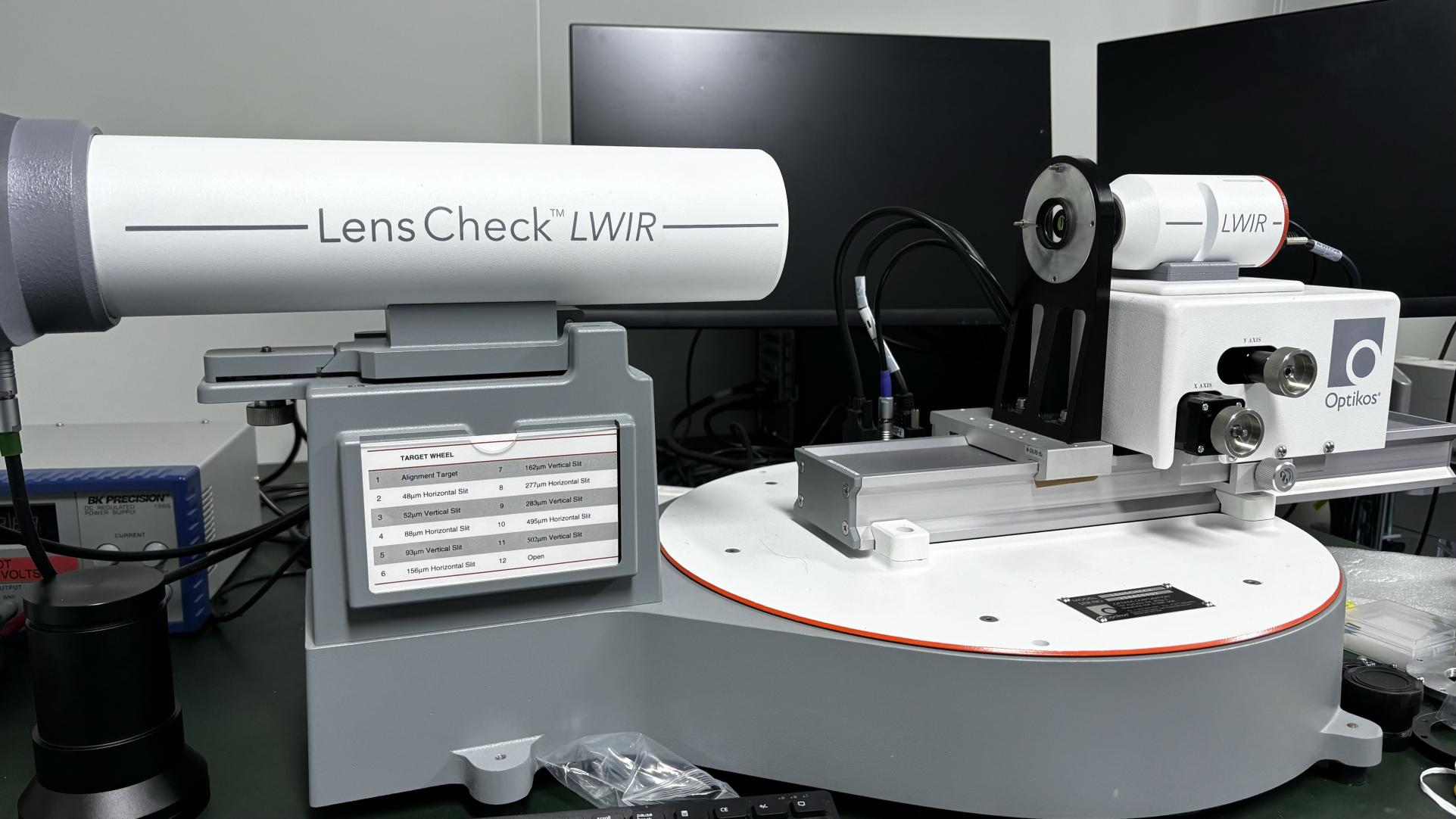
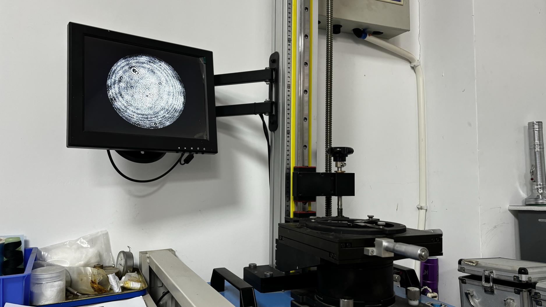
Operating in Shenzhen's advanced industrial core, Xeviora integrates German fiber laser systems with proprietary tension-testing systems. Our cleanroom ensures that temperature-induced contraction and expansion do not affect stencil dimensions. With 12 years of core technical expertise, we manage critical processes like material inspection, laser path optimization, chemical polishing, nano-coating curing, and 3D Automated Optical Inspection (AOI) under one roof.

Through our network of 850 global supply chain partners, we secure high-grade nickel and fine-grain steel coils during market fluctuations. This vertical integration allows us to offer 24-hour manufacturing turnaround for standard stencil requests, providing stable supply chains to contract manufacturers in North America, Europe, and Asia.

Technology Roadmap & Future Outlook

As the microelectronics industry targets sub-2nm nodes and multi-chip module (MCM) architectures, stencil technology must evolve accordingly. Our technology roadmap focuses on three main developments:

  • AI-Driven Aperture Modification: Utilizing deep learning models to predict solder volume requirements based on PCB board finish (HASL, ENIG, OSP), paste chemistry, and local pad layout density.
  • Additive Electroformed Nano-Stencils: Developing hybrid electroformed stencils that build custom micro-apertures directly on top of laser-cut templates. This approach helps control print heights across adjacent components with different mass profiles.
  • Real-Time Tension Sensors: Embedding digital strain gauges within the aluminum stencil frames. These sensors communicate directly with SMT printers to adjust squeegee pressure and release speeds dynamically, compensating for frame fatigue.

Global Procurement: Quality Assurance, Logistics, & Compliance

Managing global shipments of high-precision stencils requires specialized packaging and protective fixtures to prevent micro-bends and frame distortions. Xeviora ships stencils in heavy-duty, moisture-sealed shockproof crates. For system integrators and EMS partners requesting detailed documentation, we provide comprehensive QA packs including inspection files, tension measurements, and dimensional reports before dispatch.

All raw materials comply with the European Union RoHS directive, WEEE regulations, and REACH standards. This guarantees that our stencils can be safely used in green electronics production lines worldwide.

Engineering Q&A: Solved by Specialists

Q1: How do you determine the optimal aperture Area Ratio for fine-pitch BGAs?
According to the IPC-7525B standard, the Area Ratio (AR) represents the ratio of the aperture opening area to the area of the aperture walls. For circular BGAs, this simplifies to $AR = D / 4T$ (where $D$ is the diameter and $T$ is the stencil foil thickness). For stable solder paste release, the AR must remain above 0.66. If the design drops below this limit, we recommend switching to fine-grain steel foils combined with advanced chemical polishing or nano-coatings to reduce surface tension.
Q2: What is the average lifespan of your laser-cut stencils, and how can it be extended?
A standard laser-cut stainless steel stencil retains its shape for up to 80,000 to 100,000 print cycles under normal operating conditions. Applying a nano-coating layer extends this lifespan by reducing friction against the board and the squeegee blades. To maximize operational life, avoid cleaning the stencil with aggressive solvents that can degrade the nano-coating, and use squeegees with a smooth finish.
Q3: How do step-up and step-down stencils improve SMT assembly yield?
PCB designs often feature a mix of large components that need high solder volume (such as power terminals and connectors) and small, fine-pitch parts (such as micro-BGAs). Step stencils address this by varying the thickness across different zones of the foil. A step-down area reduces stencil thickness to prevent bridging on fine-pitch parts, while a step-up zone increases thickness to deposit sufficient paste on large connectors.
Q4: What is the advantage of using laser cutting over chemical etching?
Laser cutting creates clean, straight vertical walls with a natural 1 to 2-degree taper, ensuring excellent paste release. The positioning tolerance is kept under 3 microns. In contrast, chemical etching suffers from lateral undercut issues that limit its suitability for fine-pitch applications.
Q5: How does Xeviora ensure the quality and accuracy of each manufactured stencil?
Every stencil is inspected on a dedicated 3D AOI system. This equipment measures the coordinates and dimensions of all apertures against the original Gerber CAD file. Any deviation larger than 5 microns is flagged, and the stencil is rejected. We also perform regular tension checks on the mesh and frame to ensure stable registration during printing.
Q6: Which solvents and cleaning agents are compatible with your nano-coated stencils?
Our hydrophobic and oleophobic nano-coatings are fully compatible with common water-based SMT stencil cleaning agents, including isopropyl alcohol (IPA) and modified alcohol formulations. However, high-pH alkaline cleaners and strong ketones should be avoided as they can degrade the thin nano-film over time.
Q7: Can you produce stencils with specialized alignment pin holes for custom printers?
Yes, we support alignment setups for printers from manufacturers like DEK, MPM, GKG, and Ekra. Gerber CAD files must contain the tooling locations, alignment fiducials, and any custom mounting slots required.
Q8: How do fine-grain steel foils help reduce micro-solder balls during assembly?
Standard stainless steel foils have grain boundaries that can cause micro-grooves along the laser-cut walls, leading to solder paste entrapment. Fine-grain foils offer a smoother cut, reducing paste retention and preventing the release of micro-solder balls onto the PCB surface.

Optimize Your SMT Yield Rates Today

Consult with our engineers to configure your next stencil design. Send us your Gerber data for a full Design-for-Manufacturing (DFM) review and advice on optimal aperture scaling.

Complete Component & Assembly Hardware Solutions