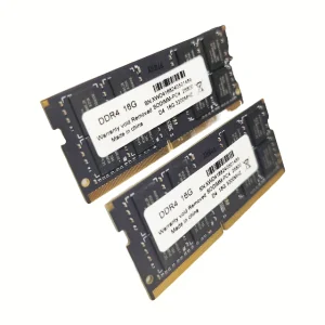
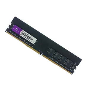
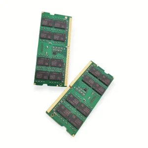
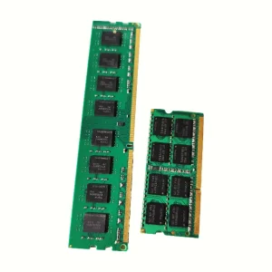
Explore our leading range of high-density interconnect PCBs, double-layer boards, thermal heatsinks, and enterprise-grade DDR4/DDR5 memory modules engineered for global technology markets.
In the rapidly evolving landscape of global technology manufacturing, finding a partner that bridges the gap between high-precision Printed Circuit Board (PCB) assembly and advanced semiconductor memory architectures is critical. Xeviora Memory Technology (China) Co., Ltd. stands at this strategic intersection. Established in 2017, Xeviora has leveraged over 12 years of industry expertise and 8 years of dedicated export experience to become a prominent supplier and exporter of CE-certified PCBs, high-performance DDR3/DDR4/DDR5 RAM, and high-efficiency thermal management solutions.
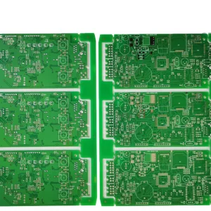
As high-speed data processing demands continue to accelerate across fields like Artificial Intelligence (AI), Edge Computing, Automotive Telematics, and Industrial Automation, the integrity of the underlying PCB layout dictates system performance. A slight variance in trace impedance, substrate thermal dissipation, or copper thickness can lead to electromagnetic interference (EMI) or severe signal degradation. By offering a unified engineering pipeline that covers custom multi-layer PCB layouts, FR4 substrate selections, and specialized high-speed memory interfaces, Xeviora provides global system integrators and OEMs with unmatched signal coherence, structural durability, and compliance guarantees.
Why regulatory alignment and rigorous verification standards are the bedrock of reliable global exports.
Our PCB manufacturing processes conform strictly to European EMC Directive 2014/30/EU. We implement optimized layout topologies, shield differential signal tracks, and utilize ground-plane optimization strategies to ensure minimal electromagnetic emission and maximum resilience to external fields.
We are dedicated to sustainable electronic design. By using high-performance lead-free Hot Air Solder Leveling (HASL) and Electroless Nickel Immersion Gold (ENIG) surface finishes, all delivered boards meet the stringent requirements of EU RoHS Directive 2011/65/EU and REACH standards.
To assure physical safety in high-power or industrial settings, our design methodologies incorporate safety creepage distances and insulation barrier controls that align perfectly with LVD Directive 2014/35/EU, mitigating hazard risks under high thermal loads.
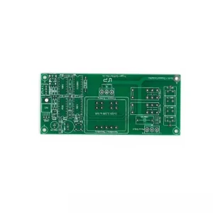
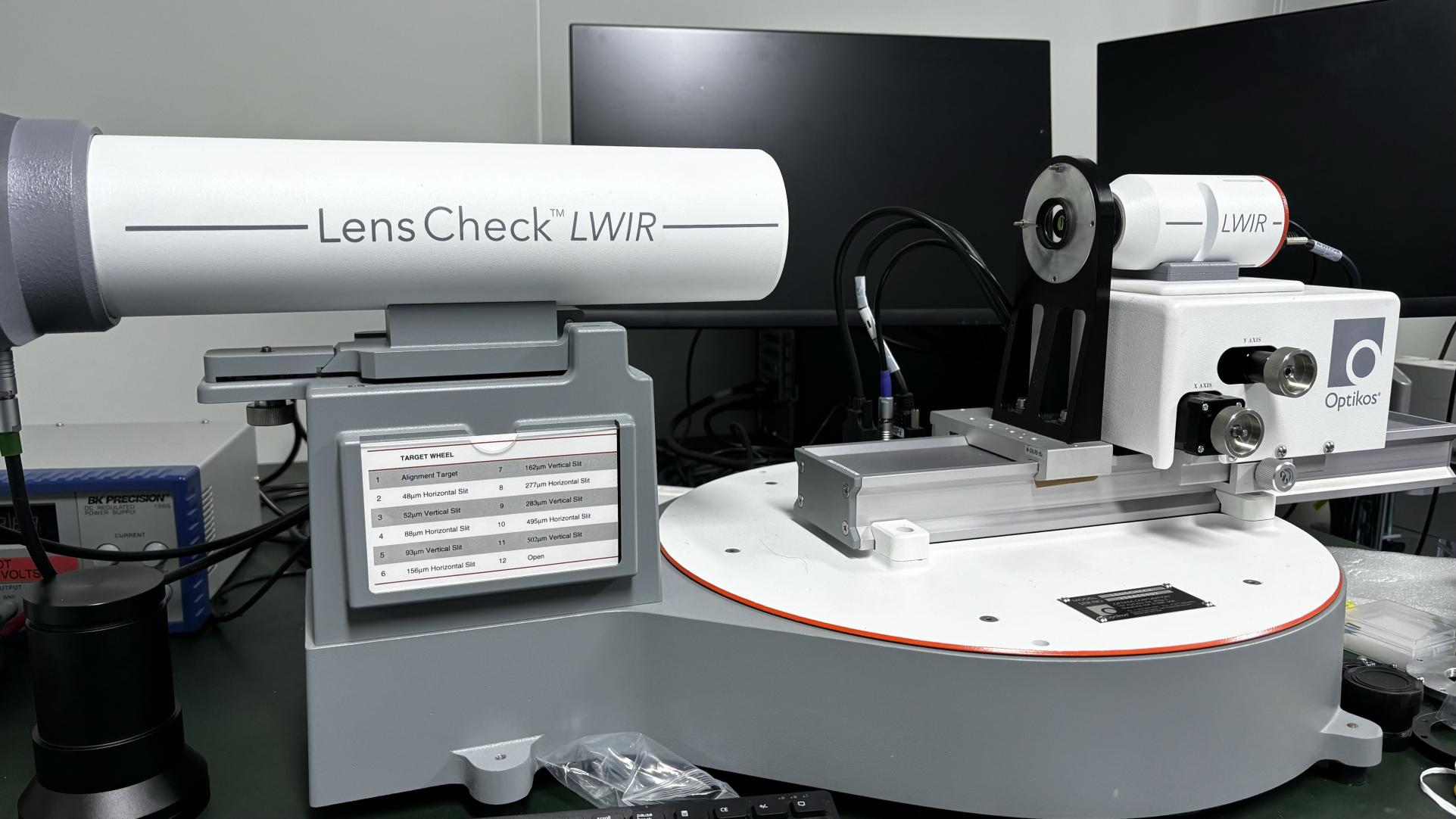
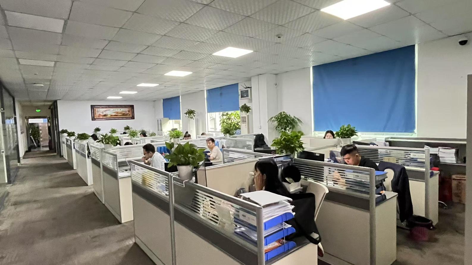
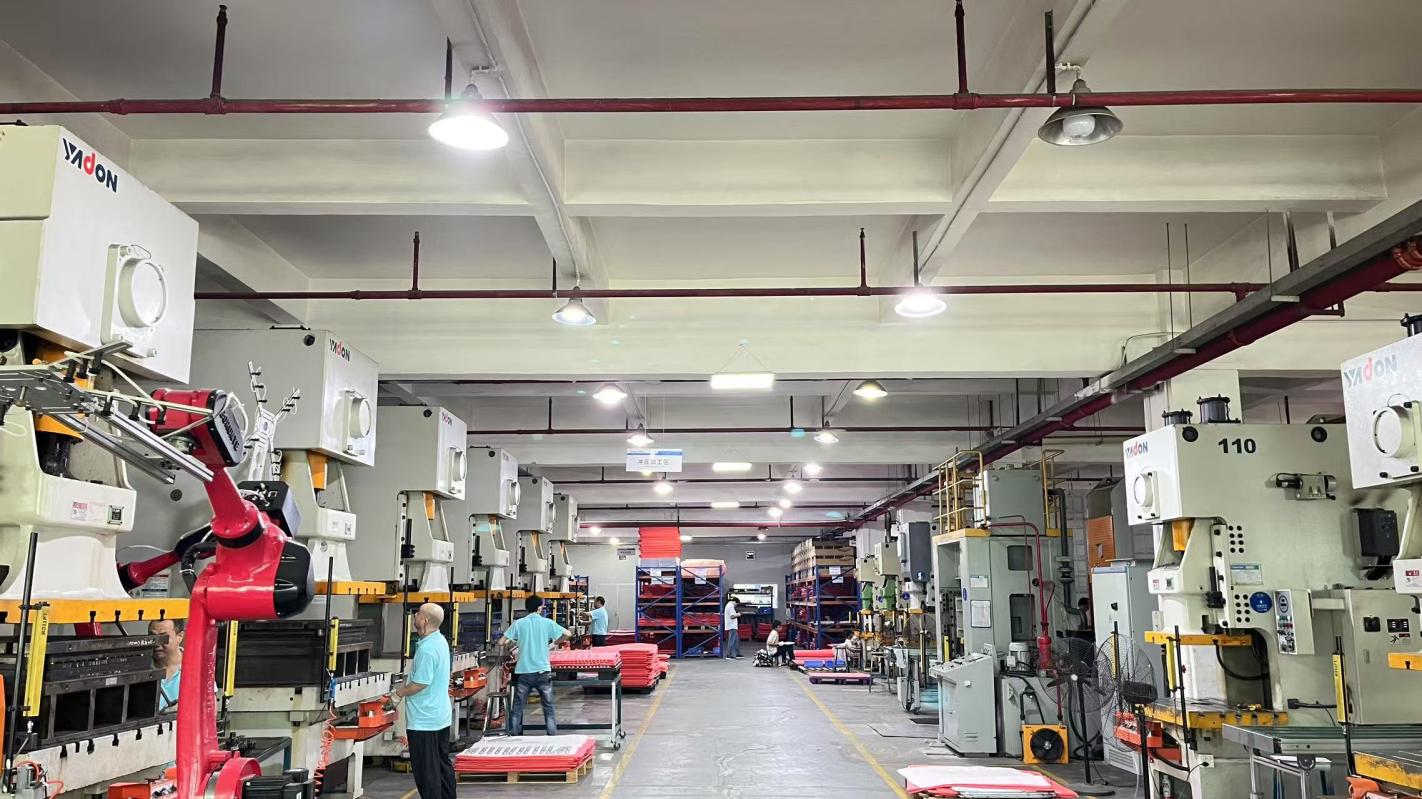
Operating out of China’s high-tech manufacturing corridors allows Xeviora to benefit from an unparalleled component sourcing ecosystem. While our localized, high-precision facility spans 368 square meters for rapid prototyping and micro-gap assembly validation, our extensive integration with over 850 verified supply chain partners globally gives us unmatched scalability.
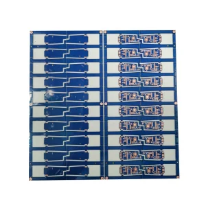
Whether a client requires a quick-turn run of 2-layer HASL PCBs for prototype evaluation or a mass production order of complex 12-layer impedance-controlled layouts paired with DDR5 SMT assembly, we maintain consistent cycle times and low unit costs. This dual capability—combining flexible high-mix, low-volume (HMLV) fabrication with high-volume production lines—provides system integrators with rapid time-to-market advantages and robust buffer stocks.

A reliable printed circuit board begins with the correct selection of materials. Standard consumer electronics often rely on low-Tg (Glass Transition Temperature) FR4 substrates, which can fail under continuous thermal stress or high vibration environments. At Xeviora, we recommend high-Tg materials (Tg170 and Tg180) for industrial applications, automotive systems, and dense server boards. These advanced materials maintain their mechanical structural integrity, low dielectric constant (Dk), and low dissipation factor (Df) even when operating under high thermal thresholds.
For RF (Radio Frequency) and high-speed data systems, trace geometry and impedance tolerance must be meticulously calculated. We use high-end software modeling to compute differential impedance (e.g., 90 ohms for USB lines, 100 ohms for Ethernet, and 50 ohms for single-ended signals). Our precision drilling machines, chemical plating baths, and AOI systems guarantee an etching accuracy with tolerances as low as ±5% on critical tracks.
| Specification Parameter | Standard Capability | Advanced / High-Precision Range |
|---|---|---|
| Layer Count | 1 - 4 Layers | 6 - 16+ Layers (Multi-Layer HDI) |
| Substrate Material | Standard FR4 (Tg 130-140) | High Tg FR4 (Tg 170/180), Rogers, Halogen-Free |
| Finished Copper Thickness | 1 oz (35 μm) | 2 oz to 6 oz (Heavy Copper for Power PCBs) |
| Min. Trace Width / Spacing | 4 mil (0.1 mm) | 3 mil (0.075 mm) for High-Density Layouts |
| Surface Finish Options | HASL, HASL Lead-Free | ENIG (Immersion Gold), OSP, Immersion Silver/Tin |
| Impedance Control Tolerance | ± 10% | ± 5% (Controlled Impedance Routing) |
| Solder Mask Colors | Green, Blue, Red, Yellow | Matte Black, Matte Green, High-Reflectance White |
Tailoring electronic infrastructure to match the exact operational conditions and regulations of international markets.
Our heavy-copper, high-Tg PCBs are engineered to withstand continuous mechanical vibrations, voltage surges, and extreme temperature cycling. They serve as the reliable backbone for programmable logic controllers (PLCs), motor drivers, and industrial sensor arrays.
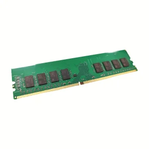
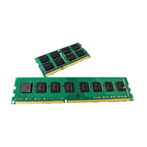
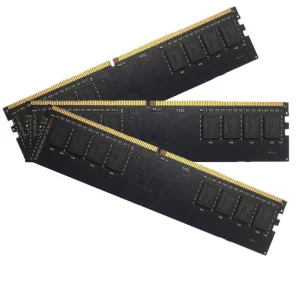
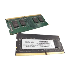
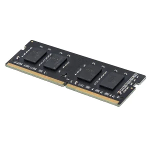
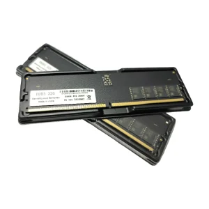
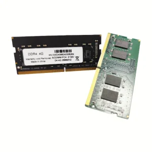
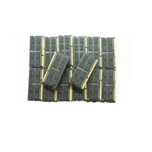
Optimized for DDR4/DDR5 high-frequency signals and BGA server chipsets. Using low-loss dielectric substrates and precision impedance matching, we ensure seamless data transfer speeds with minimal bit-error rates across bus interfaces.
Supporting high-frequency RF applications, base station circuitry, and networking switches. We provide specialized stack-ups using PTFE or Rogers hybrid constructions to guarantee minimal signal decay in gigahertz bands.
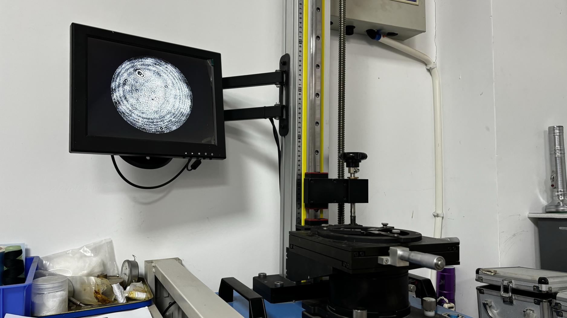
At Xeviora, we recognize that our components represent the core of our clients' products. Our QA team, consisting of 46 dedicated inspectors, operates under a multi-stage quality gate architecture. Every manufacturing batch undergoes rigorous verification steps before leaving our facility to eliminate any potential latent defects:
Answers to common questions regarding compliance, material choices, engineering support, and logistics for PCB and memory procurement.
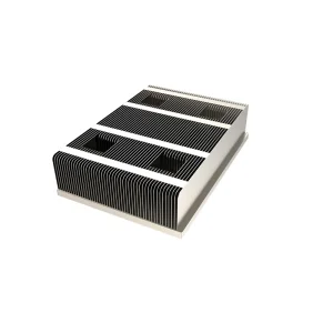
Complete your design with our high-grade amplifier modules, memory units, and custom heatsinks.